(back to mainpage)
- On the CCB there are
2 connectors for the Led-Alignment link. Which one have to be used?
- On the CCB there are
two different sets (one for type A and one for type B) of connectors for
test pulse cables. Connectors inside the same set are equivalent?
- What can be done if
one test pulse theta cable is broken and no spares are available?
- Where
can be measured (with a multimeter) voltages and threshold applied on the
front-end boards on a chamber?
- What
is the sequence of operations when the Boundary Scan Test performs the check
of Sequence Test and Sequence Reset nets?
- How
to do if , when the check of Sequence Test and Sequence Reset sometimes
fails?
- How
to interpret an error (at the MC boot level) signaled on the TP1H-L or
TP2H-L fields?
- Why
the snap/reset test sometimes performs successfully (e.g. without signal
cables or when the front-end are switched off) and sometimes fails?
- The
MC full test program fails in measuring the voltages on the Splitter Board
or when it tries to set the front-end threshold?
- How
to update the MC full test program when a newer version is up?
- Is
there the following error on the read test result?
Error: some ADC noise are equal to 3 and the error flag is
active, while some other channels are higher (e.g. channel 24 set to 26).
Moreover the voltages read on the Splitter Board are lower than expected
(e.g. Vcc = ~2.7 V , Vdd = ~1.55 , when the expected values are Vcc = ~5.1 V
, Vdd = ~2.8 ), while voltages on the front-end side are corrected (both
from the MC status and the measurement on the front-end test points).
- Has
the clock to all TRBs the same phase?
- The
PN1 switch close to the TRB-PHI clock connector is open (10 kohm) when
measured with a multimeter but the MC full test program recognizes it as
closed?
- Is
VCCin (the voltages applied with the 5V low power supply to the MC) badly
measured in the MC status data?
- Which
voltages must be applied to the Splitter Board power supplies?
- How
the front-end channels are related to the cell position into a superlayer?
- How
the front-end cables and channels are connected into TDCs channels on ROBs?
- How
the clock signal is distributed inside the MC? Concerning the clock signals
coming to different devices, which phases are fixed in hardware and which
ones can be tuned?
- When
looking at TDC status with the full MC test program, all channels are
correctly enabled (green lights) but the red error led of some TDCs in
on?
- The
ROB power or link cables have been incidentally disconnected, how they have
to be properly inserted?
(top of the
page)
ANSWERS
- Both connectors have pins connected in parallel.
Not using of the connector closer to the RPC-dedicated one is preferred for
optimizing the length and consequently the path of the cable from the CCB to
the Led-Alignment connector at the end of the MC
(top)
- For each set there are 14
connectors placed in two rows. The two connectors in every column are feed
by the same driver and the impedance of each line must be 50
ohm. Only when both connectors in the same column are connected with test
pulse cables correctly inserted to the chamber front-end, the driver works
fine. As information it should be noticed that for the chimney chambers the
number of pairs of theta test pulse cables (of the same type) is odd. Thus,
when MC is installed on the chamber, two
end-plugs (terminating the line with 50 ohm impedance) must be used
(one for type A, the other for type B).
(top)
- Test pulse theta cables are
long 3.5 meters. So, one phi cable of the same length can be used, after
being properly labelled.
(top)
- By looking at one front-end
board in such a way that signal cables (to the MC) should be inserted from
up to bottom, at the right of the connector (sky-blue colored) there are 5
test points. From left to right they are
Vdd (~ 2.5V), Vdd, Fe Width (~ 3V), Vcc(~ 5V),Threshold positive, Threshold
negative. The effective threshold applied to the front-end board is obtained by
measuring the voltage between the Threshold positive and Threshold
negative test point.
(top)
- 1)send to MC the command SelCK =7
(it selects QPLL1 e QPLL2 clock)
2)send the command SelCK=3 (it forces the microcontroller to use the clock
on-board even if QPLL1 and QPLL2 clocks are still active)
N.B.: step 1 and 2 must be done separately otherwise the microcontroller
could reset.
3) read the MC status, for checking that MC is not reset
4) perform a Jtag SAMPLE instruction on TTCrx
5) perform a Jtag Preload/EXTEST instruction on TTCrx in order to put at '0'
logical level the following nets: CKDES1,CKDES2, CK40,
TTCrdy, L1A, L1ACK. All other nets must remain to the logical value read
with the SAMPLE instruction in step 5..
6) repeat step 3.
7) set the broadcast bus to 0x08 (=sequence reset) and
strobe1 to '1', with a EXTEST instruction.
8)check that Sequence Reset read on all ICs on the Board is set to '1'.
9)set the broadcast bus to 0x80 (=sequence test ) ,
strobe2 to '1' and strobe1 to '0' , with a EXTEST instruction.
10)check that Sequence Test read on all ICs on the Board is set to '1'.
11)make a Jtag BYPASS instruction by resetting the TAP controller on TTCrx.
12) send the command SelCK=7 to the MC.
13) send the command SelCK=4 (it selects the clock from the TTC
system)
14) repeat step 3.
(top)
- If the version of the
Boundary Scan Test program is older than 4.3 sometimes can happen that
sequence test or reset are seen to logical level '1' on some ICs.
This happens because the signals are generated into a FPGA in the following
way: when the TTCrx broadcast bus is set to the properly value the signal is
generated for a given duration (about 3 us) then it is reset (for 25-50 ns)
and eventually regenerated. Thus the percentage of
test failure should be 5-10%. It is better to repeat few times the
check and to take as valid result the one which is happened more often.
If the version is newer (or equal ) than 4.3 the check is automatically
repeated up to 10 times. When the first successful occurrence happens the
test ends and, since the connection has been found, the result is positive.
(top)
- The fields TP1H-L and TP2H-L
show the the value TP1H - TP1L and TP2H - TP2L respectively. This difference
must be 1.23V +/- 1-2%. Check the value in the fields and if they are
equal to 1.23V (with a 1-2% tolerance), neglect the errror.
(top)
- When the MC is configured not
all BTIs are configured. This happens because the configuration is optimized
for data taking while, during the test of MC, BTIs are configured when
needed by the several checks. This test needs to have all BTIs configured,
thus it better to do it at last. After this test all BTIs must be
reconfigured.
(top)
- The test program fails in
measuring the voltages on the Splitter Board or when it tries to set the
front-end threshold? Check the threshold cable is completely inserted
specially on the CCB side. Sometimes this can be accidentally disconnected
when the Server Board is inserted. Check also that the threshold cable is
properly crimped.
(top)
- 1) download the updated file (Franco
Gonella communicates where it is)
2) backup the folder \test_mc where the old program is in.
3) delete everything in \test_mc except two following folders:
test data
test bsr
3) unzip the new downloaded file into a temporary folder and then copy all
files and folders into \test_mc
4) when start program for the first time, after typing the MC type
and ID, go to the setup panel, write the server IP address (the port is
18889) and save this information in the file config_def.cfg
(top)
- If ADC noise is lower than 3
it means that threshold cable is correctly connect and the Splitter Board is
switched on. If the noise is greater for a give channel, it means that
channel is floating. For example the channel 24 corresponds to the Vdd
Splitter Board. Check if threshold cable is connected or badly crimped.
(top)
- The clock of all TRB phi has
the same phase. The clock to the TRB theta is delayed in order to compensate
the different length of the phi and theta signal cables from the front-end.
The test which verifies that the clock cables length is correct is the
"BTI skew".
(top)
- When the switch is open the
net connected to the TRACOs has pulled-up to Vcc via a resistor, so that a
logical high level should be set. On some oldest TRBs the resistor has a 10
kohm value. This way a spurious voltages level is obtained (about 2V), so
that the logic level is undefined and the test can fail. The correct
solution is obtained by replacing the resistor (named R15 and placed
between Traco 3 e il Traco 2) with one having 330 ohm value.
(top)
- First of all, check the
voltages on the power supplies side (is a current limiter on? if yes, is it
properly set?). Then check voltages on the low power patch panel. Typical
values are from 0.8V to 1V higher that the nominal ones (e.g.
6V for the 5V and 4.2V for the 3.3V). Check that the other voltages read by
the MC are correct. If all voltages applied are correct the problem could be
in the CCB. In the backside PCB side respect to power connector there are
two resistors (R122 and R123) of 4.7 kohm resistance. Check this value (with
a multimeter) and if they are correctly soldered. If yes, it could be the
case of changing the CCB.
(top)
- The Splitter Board is
connected to the power with 4 cables:
Red : +2.6 V
Brown : return channel of +2.6 V (eventually connected to GND)
Blue : return channel of +5.1 V eventually connected to GND)
Grey : +5.1 V
This values are referred to the nominal and expected ones on the Splitter
Board. Voltages applied on the power supplies could be higher (due to the
voltage fall on cables). Values on the Splitter Board can be checked with a
status command send to the MC connected.
(top)
- Each front-end board (1
connector) has 16 signal channels. They are labeled in the following way.
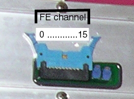
Each front-end board is connected to 16 cells within the same superlayer.
The correspondace between channels and cells is showed in the following
picture
Successive front-end board are connected to successive groups of 16 cells.
(top)
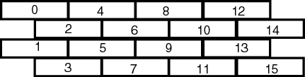
- The following picture shows a ROB how it is seen
when inserted into a MC placed into a DT chamber, keeping PHI1 superlayer at
the bottom and PHI2 at the top.
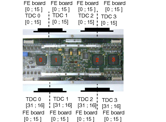
This way the bottom 2 connectors are used for signal cables from PHI1 while
the upper 2 for cables from PHI2. Each ROB connector is connected to 2
front-end board, one half connector for every front-end board. Mapping
between front-end and TDC channels is shown.
(top)
- Diagram below shows the clock distribution inside
the MC
.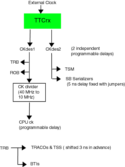
The clock signal is sent by the TTC system and received with the TTCrx IC,
hosted on the CCB inside the MC. The TTCrx has 2 clock outputs, called
CKdeskewed1 and CKdeskewed2, whose phases can be independently
delayed. The delay is set by sending the command TTC_FineDelay, whose
parameters are the channel (0 means CKdeskewed1, 1 means CKdeskewed2) and
the delay expressed in ns units. The channel CKdeskewd1 feeds the TRBs and
the ROBs. Moreover, after a frequency divisor (from 40 MHz to 10 MHz), it is
called CPUck and it is trasmitted to the Microcotroller on the SB. The CPUck
phase can be modified with an independent delay. The channel CKdeskewed2
feeds the TSM system placed on the Server Board and the LVDS serializers
which send trigger data to the Sector Collector. The phase difference
between the clock to the TSM and the serializers is fixed in hardware. The
clock into a TRB is divided in 2 lines, one for TRACOs and TSS and the other
for BTIs. The phase difference between these two lines is fixed in hardware.
Thus, only 3 independent clock lines remain: CKdeskewed1, CKdeskewed2 and
CPUck. The line CKdeskewed1 must be delayed by 4 ns. This way
the clock line which feeds TRACOs and TSS is expected to be nearly in phase
with the TSM clock, as foreseen by design for the trigger data transmission
from TRBs to SB. Due to this fact the test_serializers (implemented in the
full MC test) is performed for checking that with 0 ns delay on the
CKdeskewed2 line the trigger data transmission perfectly works. One only
free phase remains to be fixed, the CPUck. Its phase must be adjusted with
respect both to the ROB clock (see MC-RO draft user manual in the CIEMAT web
site, section 3.2.11, where interference between Jtag clock, generated by
the microcontroller and thus dependent on the CPUck, and ROB clock) and the
TRB clock, since it is used for testing trigger path emulating tracks. This
last phase is obtained with the CPUck_phase test in the full MC test
program.
(top)
- Click on the red led and look at the messages in
the bottom of the window. Check if one of these messages appears: "jtag
instruction error" or "setup or control parity error". If so,
the default value of CPUck delay is not correct for this MC, with respect to
the ROB clock (see f.a.q. 18 and MC-RO user manual n the CIEMAT web
site, section 3.2.11). In order to find a correct value, the TDC_Jtag_test
has to be performed. This test, for any TDC, loops by increasing the delay
on the CPUck line and, at each loop, it writes and reads TDC configuration,
searching for errors.. This way a range of values can be found, where CPUck
and ROB clock don't interfere. Then the TDC must be reconfigured and in the
field "CPU ck" in the Configuration panel, a correct value into
the range previously found must be put.
(top)
- Look at the following pic:
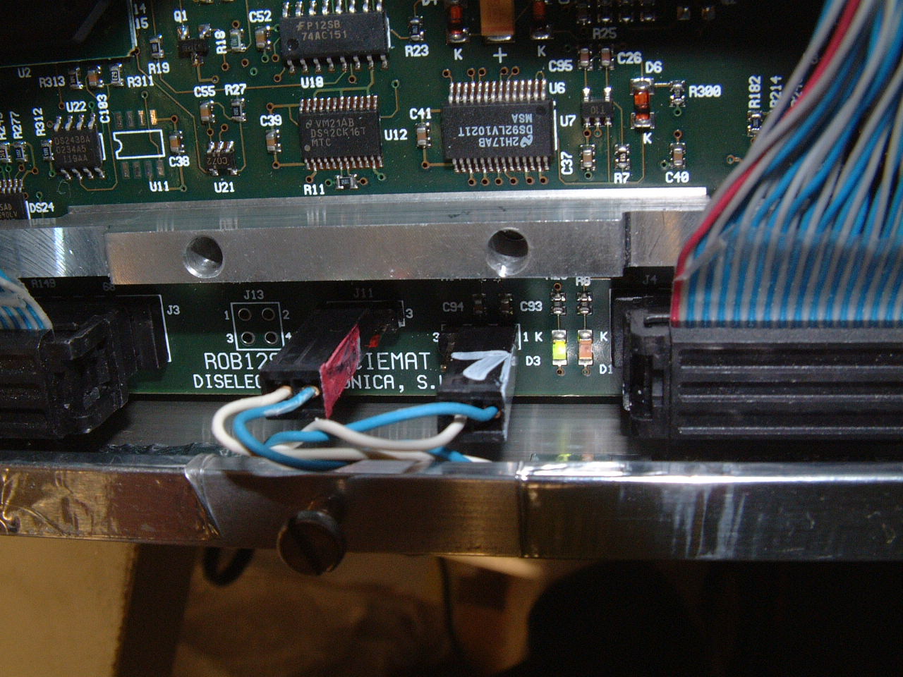
These instructions have been taken from a mail sent by Cristina (thanks!):
"the ROB clock cable is connected to the J11
connector in pins 1 and 2 and ROLINK cable to J12 pins 1 and 2. In principle
a "L" is put to the ROLINK cable to avoid confusion, and in
principle, the right side of the ROLINK connector is marked in
white and the right side the rob clock connector
in red (the blue cable should be to the right (pin 2 in ROB ck and pin1
in ROLINK))."
(top)