PageContent
NANOTECHNOLOGIES
Coordinator:
+ Fabrizio Odorici- Fabrizio Odorici E-Mail:
fabrizio.odorici@bo.infn.itLab: +39-051-2091015; Mobile: 340 2806408
Office: Irnerio
In 2001 the Bologna Section was the initiator, within INFN, of research and development in the field of nanotechnologies. The aim is to exploit the properties of nanostructured materials for applications of specific interest for the research of the Institute as well as of potential industrial interest. In fact, nanotechnologies allow the synthesis of structures on a nanometric scale or, more precisely, at sub-micrometric scales, typically less than 100 nm. These scales of magnitude anticipate the frontier of microelectronics and allow us to discover and exploit new properties of matter.
The main research activities are:
- Synthesys of nanoporous alumina.
+ Show more- Show less
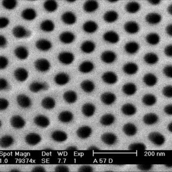
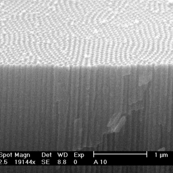
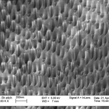
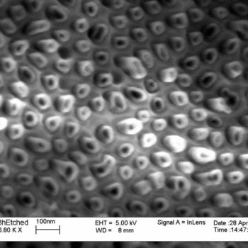
By electrochemical anodizing of aluminum it is possible to create a superficial oxide layer, with a porous “honeycomb” structure. This layer can have a thickness of between a few hundred nm, up to tens or hundreds of microns. The honeycomb structure has a variable pitch from 50 to 500 nm, which depends on the anodizing conditions, while the pore diameter is approximately equal to half the pitch. With appropriate precautions, the pore matrix can reach a very high regularity. In this way, arrays of nanopores with a high degree of order are obtained, even on a millimeter scale, which can have multiple applications: for example, they can be used as photonic crystals or as templates for the synthesis of other nanostructures, such as nanoparticles, nanowires or carbon nanotubes.
- Synthesis of metal nanowires.
+ Show more- Show less
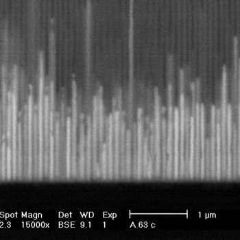
Through electroplating processes on porous alumina matrices it is possible to create metal nanowires with particular opto-electronic properties: for electromagnetic radiation with a wavelength much larger than the diameter of the nanowire and for specific resonant frequencies (in the UV-VIS-IR range ) depending on the geometry, a high absorption and the ability to transport the perturbation along the nanowire are observed, as in a light guide.
The use of metal nanowires has found various applications, for example:
-
- hyperabsorption in laser-matter interactions for the formation of plasmas of astrophysical interest.
+ Show more- Show less
The PLANETA experiment (2017-2019) investigated the production of plasma by laser ablation of nanostructured targets. Using two Nd-YAG lasers at 1064 and 532 nm wavelength, 6 ns duration pulses are fired on targets with metal nanowires embedded in a porous alumina matrix and the resulting plasma is analyzed with different detectors. The plasmas created in this way are interesting in terms of laser-nanostructure coupling, as they seem to lead to the production of a hot, dense and long-lasting plasma (hundreds of ns), such as to achieve adequate conditions for nuclear fusion and for studies of astrophysical interest.
- optimization of radiation detectors (e.g. Silicon Drift Detectors) in quantum efficiency at specific frequencies.
+ Show more- Show less
The REDSOX2 experiment (2016-2018) investigated the application of nanotechnology on SDD-type devices, in order to increase the quantum efficiency of the current detector in the UV range, for example for applications in the reading of scintillation light. In particular, the possibility of increasing quantum efficiency in the near ultraviolet range (∼ 380 nm) was verified, by the formation of a matrix of Ag nanowires with high transmittance, which is placed on the detector entrance window, above a thin ITO (Indium Tin Oxide) layer. The double layer also acts as an anti-reflecting coating. The study showed that it is possible to obtain a plasmonic absorption resonance close to 380 nm.
- electromagnetic radiation hyperabsorption (e.g. the solar spectrum) and heat transfer in industrial application.
+ Show more- Show less
A possible application has been preliminary experimented (in collaboration with a company), through a surface treatment based on matrices of metal nanowires. These matrices create a surface with very high absorption for the UV-VIS-IR spectrum, even in conditions of high power density and for long times. In the trial application it was therefore required that the high absorbance remains constant over time in highly degrading conditions.
- Synthesis of carbon nanotubes.
+ Show more- Show less
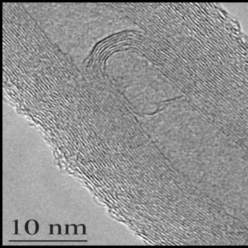
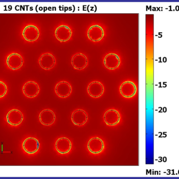
By means of Chemical Vapor Deposition (CVD) it is possible to create carbon nanotubes, with a diameter between 1 and 100 nm and length of several microns. These nanotubes show excellent electrical properties, such as high conductivity and the ability to emit electrons by tunnel effect, under the action of an electric field. They can be created in free form (freestanding) or confined in regular porous alumina matrices.
The use of carbon nanotubes has found various applications, for example:
-
- electron emitters in ion sources.
+ Show more- Show less
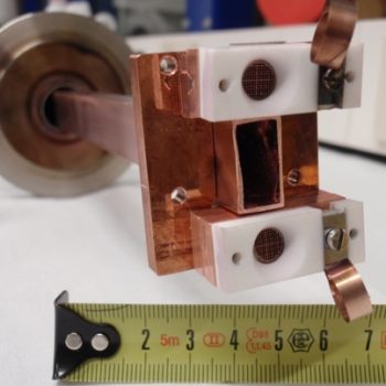
The CANTES (2009-2010) and ESOPO (2011-2013) experiments investigated the “auxiliary electron source” technique in ion sources of the ECRIS type (Electron Cyclotron Ion Source) and MDIS type (Microwave Discharge Ion Source) by means of electron guns based on carbon nanotube cathodes. In these studies, the resistance of carbon nanotubes to plasma damage was exploited to verify that in a magnetic confinement ion source the injection of auxiliary electrons is able to increase the electronic density of the plasma and the charge state distribution, and to reduce the (unwanted) concentration of high energy electrons.
- electron emitters in industrial applications.
+ Show more- Show less
Cold cathode samples were made (in collaboration with a company) for application in innovative X-ray tubes, exploiting the low beam divergence, the high miniaturization and the prompt emission of carbon nanotubes.
- high spatial resolution radiation detectors.
+ Show more- Show less
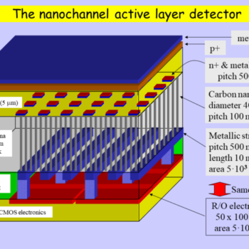
The NANOCHANT experiment (2003-2005) has investigated the realization of a ionizing particle detector with high spatial resolution, through the coupling between an active layer based on pixelated silicon junctions and an ordered matrix of carbon nanotubes acting as collectors of charge with ultra fine segmentation.
The research group: Marco Cuffiani, Luciana Malferrari, Alessandro Montanari, Fabrizio Odorici.
The collaboration: research is carried out in collaboration with various institutes, including the CNR-IMM-Bologna, INFN-LNS-Catania, INFN-Trieste and IAP-Frankfurt. The applications tested so far, in addition to electrochemical techniques, have integrated many skills, including: aspects of optics, electronics, radiation-matter interactions, plasma physics, simulation and construction of electrostatic systems for the generation and control of electron beams low energy.
Topics for thesis and master’s thesis are available (info: fabrizio. odorici@bo.infn.it).


